
In modern SoC (System on Chip) designs, the clock signal is indispensable. A precise clock is typically provided by a crystal oscillator. Due to the difficulty of integrating crystal oscillators directly into semiconductor chips, they are usually implemented as discrete components on the PCB crystal oscillator design. The role of the clock in an electronic system is as vital as a heartbeat in a human body. If a clock malfunctions, the entire system or communication channel can fail.
For instance, consider a 16 MHz crystal oscillator providing the reference clock for a 2.4 GHz Bluetooth chip. If the crystal oscillator exhibits a frequency deviation, such as -48 ppm (resulting in an actual frequency of 15.999223 MHz), the Bluetooth carrier frequency, which is a multiple of the reference clock, will also inherit this deviation. Consequently, the Bluetooth frequency could shift to approximately 2,399,883,450 Hz, introducing an offset of nearly 100 kHz. Such a deviation might cause communication failure with devices operating at standard frequencies. Therefore, designing a stable and reliable oscillator circuit is crucial.
Key Considerations for Crystal Oscillator Design
When designing a PCB crystal oscillator circuit, engineers must address three main goals:
- Minimize uncertainty from parasitic capacitance
- Minimize temperature-related variations
- Reduce electromagnetic interference (EMI) with other circuits
With over ten years of expertise in PCB prototyping and fabrication, PCBYES understands the importance of precise crystal oscillator circuit design. We consistently deliver high-quality PCB and PCBA turnkey services, catering to the most stringent demands in quality, delivery, and cost-effectiveness.
Layout Design Guidelines
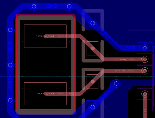
1. Place the Crystal Oscillator Close to the IC
The crystal should be close to the chip that uses the clock signal. Short trace lengths minimize signal degradation, parasitic capacitance, and crosstalk.
2. Implement Ground Guarding with Via Stitching
Surround the crystal oscillator area with ground vias to create an effective ground shield. This reduces noise and EMI susceptibility.
3. Avoid Signal Traces Beneath the Crystal
No other signal lines, especially other high-frequency clocks, should pass beneath the crystal package. Such routing can introduce noise coupling and parasitic effects.
4. Ensure Short Return Paths for Load Capacitors
Load capacitors' return paths to ground should be as short and direct as possible to maintain signal integrity.
5. Route Signal Traces Through Capacitors First
The trace from the IC output should first pass through the load capacitors before reaching the crystal oscillator to optimize matching and signal stability.
Routing Methods for Different Oscillator Packages
Two-Pin SMD Passive Crystals
1. Utilize Central Routing for Larger Packages
For crystals with larger packages, traces can be routed through the center to reduce parasitic effects.
2. Keep Test Stubs as Short as Possible
If test points are required, ensure that the stubs are extremely short to avoid introducing significant signal reflections.
3. Use Pseudo-Differential Routing
Although a real differential signal is not necessary, routing the two traces symmetrically and closely together on the same layer helps minimize noise pickup.
4. Remove Copper Below Crystal if Necessary
In certain designs, especially where frequency stability is critical, it is advisable to remove copper below the crystal to minimize parasitic capacitance and thermal effects.
5. Ground Metallic Crystal Housings
If the crystal uses a metal casing, ensure that the casing is grounded to enhance the electromagnetic immunity of the circuit.
6. Select Crystals Rated for High Temperatures
Crystals should be specified to operate at temperatures up to at least 125°C to ensure performance across industrial environments.
Four-Pin SMD Passive Crystals
The principles mentioned above also apply to four-pin SMD crystals. Additional care must be taken to properly ground any dedicated ground pins.
Special Considerations for Active Crystal Oscillators
Active crystal oscillators integrate an oscillator circuit inside the package, requiring additional attention during layout.
1. Proper Placement for Aging Test Boards
In HTOL (High-Temperature Operating Life) test setups, ICs are often placed in sockets. Crystals should not be placed on the same side as the socket to prevent increased trace lengths. Instead, they should be mounted on the opposite side with proper via connections.
2. Add Return Ground Vias near Vias Connecting to IC
When vias are used to route signals from the oscillator to the IC, return ground vias should be placed nearby to maintain signal integrity.
3. Power Filtering for Active Oscillators
Special attention should be paid to the decoupling capacitors at the oscillator’s power supply pin. Larger capacitors should be placed farther from the oscillator, with smaller capacitors positioned closer, forming a multi-stage filtering network.
The crystal oscillator circuit is a small yet critical part of any electronic system. By following systematic layout practices—such as minimizing trace lengths, guarding with ground vias, and optimizing component placement—engineers can ensure stable clock signals, improved product reliability, and reduced electromagnetic interference.
At PCBYES, with our team of seasoned electronics engineers, we are committed to delivering PCB and PCBA solutions that meet and exceed our clients’ expectations. Whether you're looking for PCB prototypes or turnkey assembly services, we pride ourselves on being your trusted partner in every stage of your PCB journey.


